
Digital electronic computer is the driving force that fuels our modern civilization. Modern computation has allowed the development of ever-increasing computing power by size scaling following the Moore’s Law. However, since the size scaling of CMOS technology has shown evidence of approaching a limit due to increased power density at small technology nodes, conventional digital computation using current von Neumann architectures and 0/1 bits will inevitably be stagnating because of these fundamental physics and material limits. Now, based on the ShanghaiTech Microelectronics Center, the Post-Moore Microelectronics and Integrated Circuit Center (PMICC) at SIST has made major progress on the novel cryo-CMOS and optoelectronics devices.
Collaborated with Dr. Hu Shaojian’s team, Prof. Kou Xufeng’s group performed experimental characterizations and device modeling on the nanoscale MOSFETs with HLMC 40 nm low-power CMOS technology. Systematic temperature-dependent ID-VGS results of NMOS/PMOS devices reveal that both the threshold voltage and the effective channel mobility exhibit strong correlations with the device size owning to the depletion region broadening around the gate channel at cryogenic temperatures. By taking the temperature-driven gate geometry effects into consideration, a generic physical model with universal fitting parameters is proposed to depict the transfer characteristics of all CMOS transistors across the device size chart, and further validations of the modified BSIM compact model might pave the way for an accurate design of cryogenic electronics applications. Such work, entitled as “Temperature-Driven Gate Geometry Effects in Nanoscale Cryogenic MOSFETs”, was published in IEEE Electron Device Letters. 1st year Ph.D. candidate Wang Zewei and 4th year undergraduate Tang Zhidong are the co-first authors. This work was sponsored by the ShanghaiTech University’s Start-up Fund, the Strategic Priority Research Program of CAS, the National Key R&D Program of China, National Natural Science Foundation of China and the Shanghai Sailing Program.
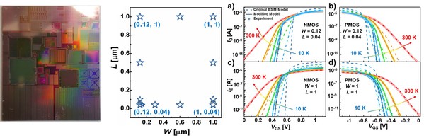
Figure 1 Generic compact device model on HLMC 40LP cryo-CMOS chip.
In another important research direction, GaN Schottky diode devices have excellent characteristics such as high electron mobility and low leakage current, which would favor the adoption of cryogenic electronics for superconducting electronics, space observatories, cryo-imaging, and future data centers. Prof. Zou Xinbo’s group proposed the modified thermionic emission diffusion (TED) mode, starting from the physical formula of conventional TED model. Considering the ideality factor will increase dramatically at cryogenic temperature, this model has been developed to explained the discrepancy of Schottky barrier height extracted by capacitance-voltage and current-voltage methods. Meanwhile, three leakage current mechanisms have been explaining and fitting J-V experimental data at various temperature ranges and bias conditions. Using deep level transient spectroscopy (DLTS) technology to obtain four traps that practically became inactive at cryogenic temperatures, thus greatly suppressing the trap-assisted carrier hopping effects. The paper entitled “Electrical characterization of GaN Schottky barrier diode at cryogenic temperatures” has been published online in Applied Physics Letters. 1st year graduate students Chen Jiaxiang and Zhu Min from Prof. Zou’s group are student authors and Prof. Zou is the corresponding author. This work was supported by ShanghaiTech University’s Start-up Fund, Shanghai Pujiang Program, and the CAS Strategic Science and Technology Program under Grant.
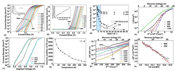
Figure 2 Forward and reverse current density-voltage characteristics of GaN Schottky barrier diode and fitting results at cryogenic temperature ranges.
In the field of interband cascade lasers, Prof. Wang Cheng’s group first proposed a rate equation model for mid-infrared interband cascade lasers (ICLs) since its invention in 1997, which is a very universal and powerful theoretical tool for studying the physics of lasers. The proposed model is of prime importance for studying physical mechanisms, laser dynamics, design and performance optimization of ICLs. In addition, Prof. Wang’s group unveiled the linewidth broadening factor of ICLs for the first time. It is found the value is smaller than that of conventional quantum well lasers, but larger than that of quantum cascade lasers. Linewidth broadening factor is a key fundamental parameter of semiconductor lasers. It determines many laser characteristics, including spectral linewidth, frequency chirp, and nonlinear dynamics. This work is very helpful for designing low-noise gas spectroscopy systems. The above work are published in IEEE Journal of Quantum Electronics with the title “Rate equation modeling of interband cascade lasers on modulation and noise dynamics”, and in Applied Physics Letters with the title “Linewidth broadening factor of an interband cascade laser”, respectively. The first author of both papers is Yu Deng, a 2nd year graduate student from Prof. Wang’s group. The above work was financially supported by NSFC and Shanghai Pujiang Program.
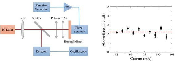
Figure 3 (a) Experimental setup for the linewidth broadening factor measurement and (b) the measured result.
Links:
https://ieeexplore.ieee.org/document/9050739
https://doi.org/10.1063/1.5131337
https://ieeexplore.ieee.org/document/8986610
https://aip.scitation.org/doi/full/10.1063/1.5123005

 沪公网安备 31011502006855号